SECTOR
Technology
Printed electronics have been studied for over 50 years. The conductive inks used in automotive windshield de-icing systems date back to the 50s, while the first printed transistors or OLEDs date back to the 80s. It’s a multidisciplinary field, drawing on skills in chemistry, physics, electronics and the machinery and equipment sector. This combination of new materials and low-cost, large-area production techniques opens up a wide range of electronic functions associated with thin, light, flexible components that can be manufactured and integrated directly into products at low cost.
At present, there are many players in this sector, operating in different sectors.
- French and European R&D skills are relatively dispersed within teams whose core business is not printed electronics, as may be the case in other European countries. Things are changing, platforms are being planned and French players are getting organized.
- Start-ups are developing specific applications and equipment based on research work.
- The chemical giants are material suppliers, developing inks and materials with the best performance characteristics. Manufacturing processes, substrates and deposited materials are interdependent elements in the production of printed components. R&D in this field is complex, as changes in one of these elements affect the other two. The share of materials in the overall manufacturing cost of an organic electronics device, for example, is between half and two-thirds of the cost. Materials (substrates and formulations) therefore represent a strategic challenge for the development of the industry.
- Different production techniques are adapted to the specific constraints and characteristics of the materials and formulations used in printed electronics. Expertise and mastery of production processes are therefore key to breaking into the printed electronics market.
- Equipment manufacturers are adapting their technologies or proposing new ones to meet the specific requirements of the materials used, large-area electronics and their various applications.
Schools and Universities
Printed electronics processes develop heating systems, sensors, actuators, antennas, transistors, capacitors, batteries, fuel cells, light-emitting diodes, photovoltaic cells and displays.
To integrate these technologies into the manufacturing processes of electronic systems, and to meet the new challenges of innovation, manufacturers need new skills. This means developing training in the context of printed electronics.
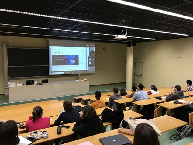

AFELIM’s ECOLES & UNIVERSITES working group has been created
A SCHOOLS & UNIVERSITIES working group has been set up within AFELIM to bring together colleges, schools and universities preparing specific modules in printed electronics. The aim is to anticipate the needs of laboratories and manufacturers, and to develop know-how in chemistry, electronics and printing.
This working group has drawn up a document outlining the specific features and know-how of the various schools. Bridges between teachers from different schools are also organized to develop appropriate trades.
CONTACT NAMES
BORDEAUX INP – Bordeaux
OLEDS, OPV, SENSORS
VIGNAU Laurence – laurence.vignau@ims-bordeaux.fr
EIDD – Paris
OLED, POV, SENSORS, TRANSISTORS
BATTAGLINI Nicolas – nicolas.battaglini@univ-paris-diderot.fr
HEPIA – Geneve
ANTENNA, RF, MEDICAL, SENSORS
Bechevet Delphine – delphine.Bechevet@hesge.ch
GRENOBLE INP – PAGORA – Grenoble
GRAPHIC PRINTING, ELECTRONIC PRINTING, GREEN ELECTRONICS
REVERDY-BRUAS Nadège – nadege.reverdy-bruas@grenoble-inp.fr
ISEP – Paris
ELECTRONICS, ROBOTICS, IA
CAMARA Mariam – mariam.camara@isep.fr
ITECH – Lyon
CHEMICALS, PAINTING, INKS
PHILIBERT Jean-Pascal – jean-pascal.philibert@itech.fr
Sophie BARNET – sophie.barnet@itech.fr
LUMOMAT – Anges, Nantes, Rennes
OPV, OLEDs, OFETs, SENSORS
Mohammed BOUJTITA (CEISAM) – Mohammed.boujtita@univ-nantes.fr
Piétrick HUDHOMME (MOLTECH – Anjou) – Pietrick.hudhomme@univ-angers.fr
Muriel HISSLER (ISCR) – muriel.hissler@univ-rennes1.fr
Laboratories
Research center for new energy technologies. Based in Grenoble and Chambéry, in the heart of France’s leading energy-producing region, the Laboratoire d’Innovation pour les Technologies des Energies Nouvelles et les nanomatériaux (Liten) is the first European research center entirely dedicated to the energy transition.
Thanks to its position within the CEA, over the past 15 years Liten has become a major player in technological research to meet the challenges of energy and the environment, while supporting economic growth.
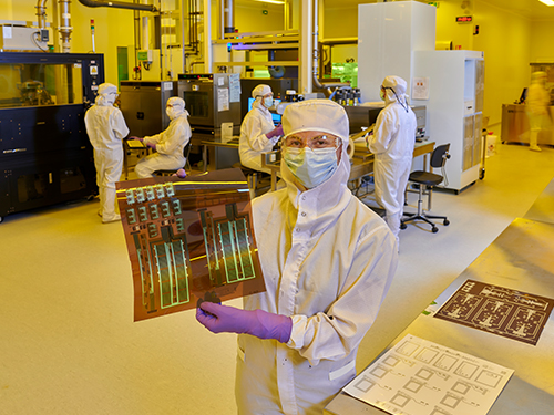
crédit CEA-LITEN
IRT ST EXUPERY
Accelerating scientific and technological research and transfer to industry in the aeronautics, space and embedded systems sectors: high-performance multifunctional materials – electric aircraft – systems engineering and modeling – intelligent systems and communications.
LCPO
The Laboratoire de Chimie de Polymères Organiques (Organic Polymer Chemistry Laboratory), based in Bordeaux, carries out polymer science research into polymerization mechanisms and macromolecular engineering.
GDR OERA
The CNRS GDR 3368 “Organic Electronics” brings together just over forty academic laboratories working in the field of organic electronics.
Materials
Substrates
The advantage of organic printed electronics is the use of flexible substrates. The choice of these flexible substrates is dictated by the drying temperatures of the different formulations printed on them.
The most commonly used substrates are PET (Polyethylene Terephthalate), PEN (Polyethylene Naphthalate) for formulations with higher drying temperature solvents. Paper and PVC substrates tend to be used for consumer applications such as tickets, packaging and smart labels.
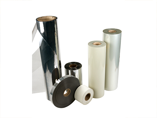
crédit ADDEV MATERIALS
Ink formulations
There are a number of different formulations currently on the market:
- Metal-based conductive inks: Ag is the most widely used metal, but its prohibitive cost is jeopardizing business models based on this metal. To replace it, formulations based on copper oxide are still being tested,
- Transparent conductors based on organic polymers used to replace transparent conductive deposits such as ITO or ZnO,
- Resistive to obtain resistive functions,
- Dielectrics to obtain capacitors, bridges, insulating zones, etc…
- piezoresistive for direct piezoresistive sensors.
Other organic polymers are also doped with p and n to produce transistors; the most commonly used are polythiophene (PEDOT-PSS), polyaniline (PANI) and polypyrrole (PP).
These different formulations have rheologies adapted to the various deposition technologies used (screen printing, flexography, inkjet, etc.).
Research is currently underway into nanoparticle-based formulations incorporating metal or graphite particles. Ongoing research is looking into the possibility of replacing transparent conductors with graphite nanotube or graphene-based formulations.
To ensure good continuity in the deposition of the ink or polymer film, the surface properties of the substrate to be printed (particularly its roughness) are of prime importance.
Ces différentes formulations possèdent des rhéologies adaptées aux différentes technologies de dépôts utilisés (sérigraphie, flexographie, jet d’encre …).
Actuellement, la recherche étudie des formulations à base de nanoparticules comprenant des particules métalliques ou graphite. Les recherches en cours permettent d’envisager le remplacement des conducteurs transparents par des formulations à base de graphite nanotubes ou de graphène.
Pour assurer une bonne continuité dans le dépôt du film d’encre ou de polymère, les propriétés de surface du support à imprimer (notamment sa rugosité) représentent des caractéristiques primordiales.
Encapsulants
Organic materials are particularly sensitive to water, steam and high temperatures, which means they need to undergo certain (often costly) treatments in order to be encapsulated. There is still a great deal of progress to be made in this field in terms of treatments and deposition techniques, in order to optimize the performance of organic applications over time.
Processes
Highly homogeneous material conductivity across the entire surface is essential for proper component operation. Material deposition must therefore be perfectly uniform, and ink film thickness, substrate type, resolution, pressure and production speed all need to be parameterized.
Screen printing
This process deposits a film of ink between 20 and 100 µm thick, and achieves good conductivity results on a wide variety of substrates. While it guarantees excellent repeatability, it is a slow process, cost-effective for small quantities with low resolution.
Flexography
Flexography allows a linearity of 60 lines per centimeter, with a thin plate of high hardness, making it ideal for electronic printing. The thickness of the ink film deposited can reach 6 to 8 µm. The disadvantage of this process lies in the profile of the deposited ink film, which creates a halo at the edges, leading to a thickness irregularity that can disrupt printing.
Flexography is used to produce RFID antennas on labels using silver inks, as well as for printed batteries. The progress made in recent years and the improved conductivity of the inks used make flexography one of the most promising techniques.
Rotogravure
Rotogravure is an intaglio printing process. This process deposits a relatively thick film of ink, ideal for electronic component applications.
Vacuum evaporation
Vacuum evaporation and spin-coating techniques are regularly employed. However, their low yield (75% of the polymer solution is lost) and high cost make them unsuitable for continuous production.
Slot Die
This deposition process is a non-contact direct transfer process compatible with all inks.
Offset printing
Offset printing is a well-established process for a multitude of substrates (paper, cardboard, metal, plastics). The resolution achieved is excellent, production speed is attractive and, last but not least, recto/verso printing produces circuits on both sides of a substrate. However, offset also has its drawbacks. To compensate for the lack of conductivity due to the thinness of the ink film (2 to 3 µm), it is generally necessary to apply several layers. In addition, a conductive ink with a viscosity of between 5 and 50 Pa.s is required, which is difficult to achieve with conductive polymers. This is why conductive metallic inks are still the main choice.
Inkjet
Inkjet is the only direct-write digital printing process: only the quantity of ink required is applied directly, under computer control, without the need for tools or contact. It is mainly used with polymer inks, as there is less risk of nozzle clogging, but metallic and ceramic ink formulations based on nanoparticles are also available.
When it comes to printing electronic components, inkjet can pose difficulties, as the positioning of the droplet is not always perfect and can lead to offsets if the process is not mastered. However, the printhead development roadmap suggests that this drawback will be minimized in the medium term. It’s an interesting technique, flexible, multi-material, multi-layer (3D) and easy to implement, even if it’s not as fast as some other unwinding techniques. Its use in industrial applications for mass markets is more complex to implement, but inkjet printing offers major technological breakthroughs for high value-added markets (specific components and customs), where it is necessary to manufacture many small series of different components.
Digital printing: aerosol printing
Aerosol jet printing enables the selective deposition of materials (conductive, dielectric, biological, etc.) on a micrometric scale on any substrate, whether planar or non-planar, flexible or three-dimensional.
Vacuum deposition
Vacuum evaporation and spin-coating techniques are regularly employed. However, their low yield (75% of the polymer solution is lost) and
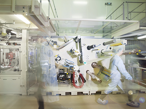
crédit ARMOR-Group
Equipments & Services
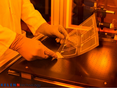
AFELIM’s EQUIPMENT & SERVICES working group brings together equipment manufacturers and service companies involved in printed electronics. The aim is to anticipate the needs of laboratories and manufacturers, and to develop the complementarities of equipment suppliers in major projects, with a view to rapidly supplying innovative new products.
The working group is preparing a booklet presenting the different functions of the printed electronics process and the know-how of equipment manufacturers and service companies.
crédit KELENN Technology
Technology platforms
“The printed electronics revolution is underway. This technological breakthrough will profoundly disrupt many economic sectors, and offer major development opportunities for innovative companies,” says Evangéline BENEVENT, President of the Commission.
To meet these technological challenges, a number of private and academic research centers, sometimes in symbiosis or under contract with manufacturers, are developing and testing new processes and equipment. And to bring value-added products to market in a short space of time, start-ups need technical resources and industrial processes that are often beyond their capabilities.
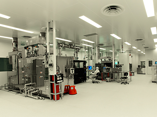
This is why France has set up several technology platforms to develop synergies around the integration of intelligent objects. These complementary platforms cover the entire sector (materials, formulations, processes, components, systems), providing specific processes and equipment for pre-production testing.
crédit photo CEA
A TECHNOLOGICAL PLATFORMS working group has been set up within AFELIM.
This group supports the development of these platforms and technical centers, and federates resources for rapid application development.
The first AFELIM booklet lists skills and know-how, resources and access to five French platforms: ELORPRINTTEC in Bordeaux, CTP in Grenoble and Douai, CT IPC in Oyonnax, SPRINT IM2NP in Marseille, PTIC CEA LITEN in Grenoble.
Le savoir-faire et la maturité technologique des plateformes :

TRL 1 Observation of the basic principle
TRL 2 Technological concept formulation
TRL 3 Experimental proof of concept
TRL 4 Technology validation in the laboratory
TRL 5 Technology validation in real-life environment
TRL 6 Technology demonstration in real environment
TRL 7 Prototype-scale system demonstration in operational environment
TRL 8 Qualification of a complete system
TRL 9 Real system demonstrated in operational environment
Members of the Technology Platforms Committee:
- SPRINT – IM2NP BENEVENT, Evangéline, Présidente
- ELORPRINTTEC, SMAAL Wiljan
- PICTIC – CEA LITEN, GALLAIRE Didier
- CENTRE TECHNIQUE DU PAPIER, LENGLET Laurent
- CT IPC, TENCHINE Lionel
Circular Economy
Printed electronics provide opportunities for innovation and differentiation for new generations of functions and products.
Production processes, at ambient temperature and air, are based on additive deposition of very thin materials, and involve a reduced number of steps. This industry generally uses clean rooms that consume very little electrical energy and water.
Printed electronics contribute to environmental impact in all market sectors :
- in transport, less weight and therefore less consumption, more functionality in a reduced volume.
- in construction, easy integration into existing environments.
- in agriculture, flexible photovoltaic films that can be integrated into greenhouses.
- in luxury goods, intelligent, recyclable packaging.
- in healthcare, traceability of medicines at lower cost.
Companies manufacturing products based on organic electronics attach great importance to environmental aspects.
Printed electronics leave a small carbon footprint: the manufacturing process relies on solutions employed at room temperature and in ambient air, using materials that can be transformed into solution.
The industry generally uses class 10,000 cleanrooms, which consume little electricity or water. Manufacturing processes are based on the deposition of materials with a thickness of only a few tens of nanometers (i.e. very small quantities of material), and also involve a reduced number of steps (typically 5 to 6).
In addition, printed electronics use plastic (potentially recycled or cellulose-based), glass substrates or non-toxic materials.

A CIRCULAR ECONOMY working group has been set up within AFELIM
AFELIM schools, laboratories and industrialists are now meeting on a regular basis to work on the subject of the circular economy in the printed electronics value chain. More than twenty members took part in this first meeting.
The expectations of this CIRCULAR ECONOMY working group are essentially to exchange information in order to provide concrete solutions, federate the common interests of AFELIM members and develop collaborative projects.
The aim is to structure a global approach and rapidly establish an inventory of recycling and life-cycle analysis of the value chain: materials, substrates, processes, products (end-of-life, recyclability, reuse of materials and substrates, etc.) in order to introduce the circular economy right from the product design stage.
